Special Feature I
![]() Home > Special Feature I
Home > Special Feature I
Future Semiconductor Technology Lab
Professor Kim, Kyung Min
1. Vision
Semiconductor technology is our future, and its innovation relies on the creative
new idea. Our vision is introducing such creative new technologies enabled by memristor into the world and leading the future.
2. Mission
Our goal is providing a complementary solution to the future semiconductor technology. In this regard, we develop high quality and high-performance memristor materials and their processes. Furthermore, we expand our research topics to the fundamental area and applications. We explore the physical origins of the memristive behaviors to find the critical solutions from them. Also, we develop new applications of memristors to shed light on the future semiconductor technology.
3. Research Fields
-
Fundamental studies of memristive physics
Exploring the nature of memristive behaviors in various materials
Discovering new memristive physics
Troubleshooting the critical issues in memristors through the fundamental understanding.
-
Emerging Semiconductor Processes for Memristors
Developing precise, reliable and well-controlled thin-film processes for the high-quality memristors.
Integrating memristive devices
-
Future Semiconductor Devices
Developing new semiconductor devices enabled by memristors such as non-volatile memory, in-memory logic, and neuromorphic computing devices
Suggesting new algorism and paradigm of computing devises based on our signature memristor materials.
4. Homepage

Nano/2-Dimensional Materials Lab (N2ML)
Professor, Kibum Kang
1. Vision
Our group aims at interdisciplinary research to improve both fundamental material science and practical applications
2. Mission
We are exploring innovative processes based on atomic-level (sub-nm) engineering techniques for manufacturing next-generation semiconductors.
3. Research Fields
-
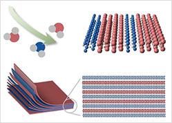
New Materials Growth
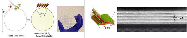
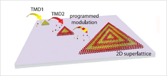
Synthesizing high quality wafer-scale monolayer transition-metal dichalcogenides (TMDs)
Finding an optimal combination of TMDs for optical device fabrication and develop a method to synthesize the material.
-
Atomic Level Engineering of Semiconductors
Designing layer-by-layer material forming vertical and lateral Van der Waals heterostructure
Studying manufacturing process that can be compatible with conventional materials and two-dimensional materials.
-
Novel Device Design
Developing paper-like semiconductors, liquid/semiconductor interfaces, MEMS
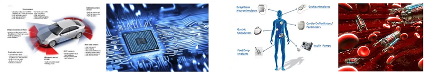
Designing sensor for self-driving car and healthcare system, Internet of Things(IoT)
4. Homepage